alb10749322
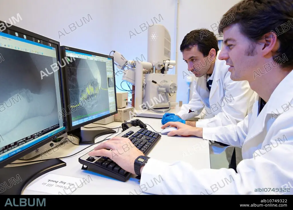
Analysis of nanostructures and nanodevices using SEM, Environmental scanning electron microscopy Laboratory, ESEM, Microscope Quanta TM 250 FEG, High-resolution surface imaging, Investigation of wet and dielectric samples, Nanofluidic phenomena, Surface chemintry in various gas mixtures, CIC nanoGUNE, Nanoscience Cooperative Research Center, San Sebastian, Donostia, Gipuzkoa, Euskadi, Spain.
| Share |
|---|
 Pinterest Pinterest |
 Twitter Twitter |
 Facebook Facebook |
 Copy link Copy link |
 Email Email |
|
Add to another lightbox |
|
Add to another lightbox |


Buy this image.
Select the use:

Caption:
Analysis of nanostructures and nanodevices using SEM, Environmental scanning electron microscopy Laboratory, ESEM, Microscope Quanta TM 250 FEG, High-resolution surface imaging, Investigation of wet and dielectric samples, Nanofluidic phenomena, Surface chemintry in various gas mixtures, CIC nanoGUNE, Nanoscience Cooperative Research Center, San Sebastian, Donostia, Gipuzkoa, Euskadi, Spain
Credit:
Album / Javier Larrea
Releases:
Model: Yes - Property: Yes
Rights questions?
Rights questions?
Image size:
5301 x 3534 px | 53.6 MB
Print size:
44.9 x 29.9 cm | 17.7 x 11.8 in (300 dpi)
Keywords:
ADULT • ADULTS • ANALYSIS • CIC NANOGUNE • COLOR IMAGE • COLOUR IMAGE • DISCOVERER • ENVIRONMENTAL SCANNING ELECTRON MICROSCOPE • EQUIPMENT • EXPLORER • GEAR • HORIZONTAL • IMAGE • IMAGES • INDOOR • INDOORS • INTERIOR • LAB COAT • LAB • LABORATORIES • LABORATORIO • LABORATORY • LABORATORY; LAB • LABS • LOOK • LOOKING • MALE • MAN • MEN • PEOPLE • RESEARCH & DEVELOPMENT • RESEARCH AND DEVELOPMENT • RESEARCH • RESEARCHER (MALE) • RESEARCHER • RESEARCHERS • RESEARCHING • SAMPLE • SAMPLES • SCANNING ELECTRON MICROGRAPH • SCANNING ELECTRON MICROSCOPE • SCIENCE AND TECHNOLOGY • SCIENCE • SCREEN • SCREENS • SMOCK (WORK) • SPAIN • TEAMWORK • TECHNOLOGY • TWO PEOPLE • WHITE COAT • WHITE COATS
